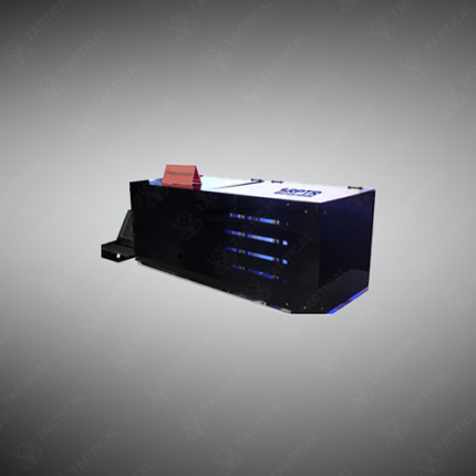
Lithography Equipment
Lithography Equipment patterns microscopic circuit designs onto semiconductor wafers, printed circuit boards, and microelectromechanical systems (MEMS) substrates by selectively exposing a light-sensitive photoresist coating to a defined energy source through a patterned mask or programmed beam path. Semiconductor fabrication facilities and microelectronics manufacturers rely on lithography systems because the technique defines the minimum feature size and overall device density achievable on a given wafer. Therefore, lithography resolution directly determines how many transistors or circuit elements a manufacturer can pack onto a single chip.
Photolithography systems use ultraviolet light projected through a photomask to transfer circuit patterns onto photoresist-coated wafers. Deep ultraviolet (DUV) systems operating at 193nm wavelength achieve minimum feature sizes down to approximately 38nm using immersion lithography techniques. Furthermore, extreme ultraviolet (EUV) lithography systems operating at 13.5nm wavelength push minimum feature sizes below 10nm, enabling the most advanced logic and memory chip nodes currently in production.
Electron beam lithography (EBL) systems use a focused electron beam to directly write patterns onto resist-coated substrates without requiring a physical mask. Consequently, EBL serves research and prototyping applications, mask-making processes, and low-volume specialized device fabrication where mask costs would be prohibitive for small production runs. Resolution on EBL systems reaches below 10 nanometers, exceeding optical lithography capability at significantly lower throughput.
Stepper and scanner systems control wafer stage positioning with nanometer-level precision during repeated exposure cycles across the wafer surface. Additionally, overlay accuracy between sequential lithography layers must remain within a few nanometers to ensure proper alignment across the multiple processing steps required to build a complete semiconductor device.
In Pakistan, lithography equipment serves semiconductor research institutions, university microelectronics departments, MEMS device prototyping facilities, and defense electronics research programs developing custom integrated circuit capability. Tactical Supply Pakistan supplies Lithography Equipment for semiconductor research, MEMS fabrication, and microelectronics procurement across Pakistan.
Showing the single result