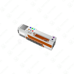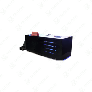


Contact-Type Exposure Machine
A high-precision photolithography system for direct mask-to-substrate contact, enabling fine-feature patterning for semiconductor, MEMS, and optoelectronic applications.
Key Features:
✔️Direct-contact exposure for accurate pattern transfer onto photoresist layers
✔️Minimum line width of 800 nm for high-resolution microfabrication
✔️Compatible with a wide range of positive and negative photoresists
✔️Integrated LED light source with 365 nm, 380 nm, and 395 nm wavelengths
✔️Step-and-repeat operation supporting 4–8 inch wafers
✔️High alignment accuracy of 0.3 μm for precise layer registration
✔️Compact and user-friendly design for efficient operation
✔️Suitable for semiconductors, MEMS, optoelectronics, PCBs, RF/microwave devices, and diffractive optics
Contact-Type Exposure Machine
Contact-Type Exposure Machine utilizes direct contact photolithography where mask plates physically touch photoresist layers on substrates for pattern transfer. The system integrates a LED light source with three wavelength options: 365nm, 380nm, and 395nm for compatibility with various positive and negative photoresist formulations. Resolution reaches 3μm minimum line width with alignment accuracy of 0.3μm for precision pattern reproduction. The unit measures 170 cm × 130 cm × 180 cm and accommodates 4-inch, 6-inch, and 8-inch wafer sizes.
Contact exposure methodology eliminates optical projection systems, enabling straightforward equipment design with reduced maintenance requirements. The mask-to-substrate interface ensures one-to-one pattern scaling without demagnification or optical aberrations. LED illumination provides stable intensity output across the exposure field while minimizing thermal effects on photoresist materials. Multi-wavelength capability allows optimization for different resist sensitivities and substrate materials without hardware modifications between production runs.
Semiconductor fabrication facilities deploy the Contact-Type Exposure Machine for prototype development and small-batch production requiring micron-scale features. MEMS manufacturers use it to pattern sensor structures and microfluidic channels in silicon and glass substrates. Printed circuit board producers create high-density interconnect patterns for RF and microwave devices operating at millimeter-wave frequencies. Optoelectronics companies fabricate diffractive optical elements and waveguide structures for photonic integrated circuits.
Tactical Supply Pakistan offers this lithography system to research institutions and production facilities requiring precise pattern transfer capabilities without the complexity of projection-based exposure equipment.
Can this machine process different wafer sizes without reconfiguration?
Yes, the system handles 4-inch, 6-inch, and 8-inch wafers through adjustable substrate holders, allowing multi-format processing within the same production environment without tooling changes.
- Fast Shipping: We partner with reliable delivery services to make sure your order gets to you quickly. We work hard to ensure every package arrives safely and on time.
- Quick Processing: Your order is processed and prepared for shipping within 24 to 48 hours. This allows us to send it out to you as fast as possible after your payment is confirmed.
- Tracking: Once your order is on its way, we will provide you with a tracking number. You can use this number to easily follow your package's journey and know exactly when it will arrive.
- Nationwide Delivery: We offer delivery to all locations across Pakistan, including major cities and remote areas. No matter where you are, we can get your order to you.
At Tactical Supply Pakistan, our relationship with you doesn't end after a sale. We are dedicated to making the long-term performance and reliability of our high-quality tactical and supplied equipment. Our commitment is to provide you with seamless support and peace of mind.
- Free Installation: We'll set up your new equipment for you, so it's ready to go. You can focus on your work while our engineers handle as per the guidelines for manufacturer.
- Maintenance: We offer quick replacements where necessary, to keep your gear in top condition. Our team will make sure your equipment is always ready when you need it.
- Customer Support: We're always here to help. Our support team is available to answer your questions and assist you long after you've made a purchase.
- Planned Preventative Maintenance: Our service includes preventative maintenance to keep your equipment in peak condition and prevent future issues.
HAVE QUESTIONS?
Fill out the form, and our team will respond promptly to assist with your product inquiries or order support.