Sheet Resistance Measurements
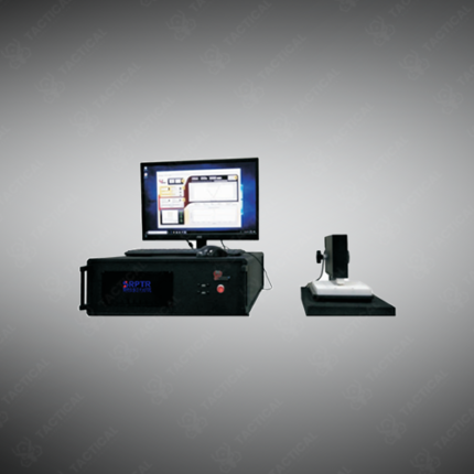
Sheet resistance measurement equipment checks how well a thin conductive layer, such as a coating, film, or semiconductor wafer surface, carries electrical current across its width. A four-point probe head touches the material’s surface, passing a known current through two outer probes while measuring voltage drop across two inner probes. This method avoids contact resistance errors that a simple two-point measurement would introduce, giving a more accurate reading of the material itself.
Probe spacing typically stays fixed at 1mm to 1.5mm between each point, with spring-loaded tips maintaining consistent pressure against the sample surface for repeatable results. Measurement range covers resistance values from a fraction of an ohm per square up to several megohms per square, depending on the material tested, from highly conductive metal films to lightly doped semiconductor layers. Most benchtop units display results directly in ohms per square, the standard unit for this measurement, alongside temperature readings since resistance shifts slightly with ambient temperature changes.
Sample size accepted by most systems ranges from small coupon pieces a few centimetres across up to full wafers 200-300mm in diameter for semiconductor industry testing. Some systems add automated mapping, moving the probe across multiple points on a single sample and building a resistance map showing uniformity across the surface rather than a single spot reading. Data output through USB or RS-232 lets results export directly into a spreadsheet or quality control database for record-keeping.
Solar panel manufacturers use sheet resistance measurement to check conductive coating uniformity across panel surfaces during production. Semiconductor fabrication facilities use it to verify doping consistency across wafer batches. Research labs working on thin-film materials also rely on this equipment to characterize new coating formulations before scaling up to production.
Tactical Supply Pakistan supplies sheet resistance measurement equipment to solar panel manufacturers, semiconductor facilities, and research labs across Pakistan. Probe configuration and sample size compatibility are matched to each buyer’s testing needs.
Showing the single result